Research
Investigating Nanoscale Materials Functionality
The Balke Research Lab investigates the functionality of nanoscale materials, with a focus on electromechanical coupling, ionic transport, and solid–liquid interface phenomena. By combining advanced atomic force microscopy (AFM) with multi-modal characterization, our team connects fundamental nanoscale processes to macroscopic material performance in energy and information technologies.
Coupling and Control Over Polar Properties

Polar Properties Explained
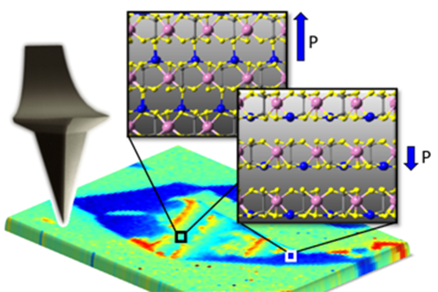
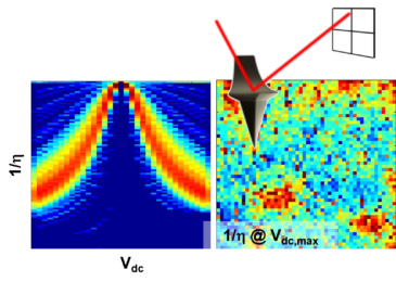
Polarization of materials is at the heart of many applications in energy and information technology, often based on the possibility of controlling polarization through externally applied forces. The action of an electric field, in particular, enacts both linear and non-linear dielectric responses, creating a rich phenomenology of dipolar glasses, paraelectrics, relaxors, antiferroelectrics, and ferroelectrics. New and unexpected properties can emerge through the coupling of or transition between distinct polar behaviors, including the possibility of changing polar material properties on demand between states of materials that typically do not coexist.
One way to realize this is the stabilization of out-of-equilibrium polar phases, often confined to interfaces or surfaces due to broken symmetry, but which are topologically protected. Of fundamental interest are not only intrinsic but also extrinsic polar phenomena, which are associated with polar properties introduced by ionic defects, which can be controlled via chemical modification routes. The project goal can only be achieved through the fundamental understanding of polar properties and how to transform them on multiple length scales, from the atomic to micrometer scale properties, which require the development of new probing methodologies and integrated microscopic approaches.
Specifically, this includes (a) polar transitions based on order-disorder phenomena in ferroelectric ion conductors such as CuInP2S6, (b) the coupling of intrinsic and extrinsic polar properties, for example, the coupling of intrinsic polarization with oxygen vacancies, and (c) the creation of new functionality at boundaries of dissimilar polar properties. The discovery of new phenomena is enabled through the quantification of AFM measurables and the extraction of polar material properties, for example, the piezoelectric constant, to allow for integration with theory.
Highlights
Brehm, J. A. et al. Nature Materials 19, 43–48 (2019).
Tselev, A. et al. Advanced Materials Interfaces 2, (2015).

Local Insights Into Electrochemical Processes

Electrochemical Processes Explained
Electrochemically induced ion insertion is the key phenomenon involved not only in different electrochemical energy storage devices, including batteries, electrochemical double-layer capacitors, and pseudocapacitors, but also in electrochemical actuators, neuromorphic computing, and electrochemical water desalination. The ion-hosting electrode most often undergoes significant volume changes driven by Coulomb interactions, bond length changes, or phase changes, which is described as electro-chemo-mechanical coupling. Understanding the mechanical response of an electrode during electrochemical cycling and its correlation to the device’s electrochemical performance and stored charge is crucial to improving the performance of insertion-type energy storage devices, electrochemical actuators, water purification, ion separation, and neuromorphic computing applications.
AFMs can be used to track local volume changes in situ and can, therefore, be used to study local electrochemical processes on the level of single grains or electrode components, which is not possible with current-based characterization techniques. One of the goals of this research direction is to build a library of strain-charge coupling phenomena for different electrochemical energy storage devices and explore the consequences of local heterogeneity of electro-chemo-mechanical on electrochemical performances and local ionic transport.
Specifically, electrode volume changes and stiffness changes as a result of (a) electric double layer formation, as well as (b) surface and (c) bulk redox processes, are investigated. Of high interest are layered electrode materials since they allow for fast ionic transport, have an interlayer space that can be modified, and typically accommodate strain without mechanical degradation, such as crack formation. Using an AFM, local current-strain coupling coefficients can be identified and correlated with information about individual grain orientation and can be directly compared to in-situ X-ray studies, which track the volume changes on the unit cell level.
Highlights

Balke, N. et al. Nano Letters 2012, 12 (7), 3399–3403.

Tsai, W.-Y. et al. Nano Energy 81, 105592 (2020).

Solid-Liquid Interface-Driven Functionality

Solid-Liquid Interfaces Explained
The structure of electrical double layers (EDL) at electrified interfaces is of utmost importance for electrochemical energy storage as well as printable, flexible, and bio-electronic devices, such as ion-gated transistors. Ionic liquids (IL) have attracted considerable attention not only due to their large electrochemical window but also due to the high energy charge density they can provide.
This is, for example, used to modify the current-voltage characteristics of metal oxides due to electrostatic doping or modification of oxygen vacancy concentrations. While this is explored on the device level, connections to the molecular-level structure of the EDL are largely missing. An important consideration is the existence of defects in the ion layering observed in the EDL of IL and its consequences for charge storage or gating properties. Since an AFM probe is sensitive to the mass density changes when approaching the solid interface inside the liquid, this approach can be used to image the EDL structure and map it in three dimensions under in situ operation of electrochemical capacitors or gated transistors.
This approach shines a light on the correlation of molecular length scale processes and the macroscopically measured device performance. This concept can be expanded to use solid-liquid interfaces to modify polar materials and their functionality. The use of a liquid provides a well-defined chemical potential at the solid-liquid interface, which can provide additional screening mechanisms for polar materials, such as ferroelectrics. The use of a liquid has the advantage of electrochemical control of surface chemistry and thus order parameter tuning.
Since AFM can be used to study piezoelectric and ferroelectric properties in liquid, this platform offers a unique opportunity to link the interfacial structure of the liquid and underlying polar properties..
Highlights

J. M. Black et al. Nano Energy 2015, 15, 737.

W.-Y. Tsai et al. Nano Energy 2019, 60, 886.

J. M. Black et al. ACS Applied Materials & Interfaces 2017, 9, 40949.