
Welcome to the Wide-Bandgap (WBG) Lab
Advancing Electronic Materials
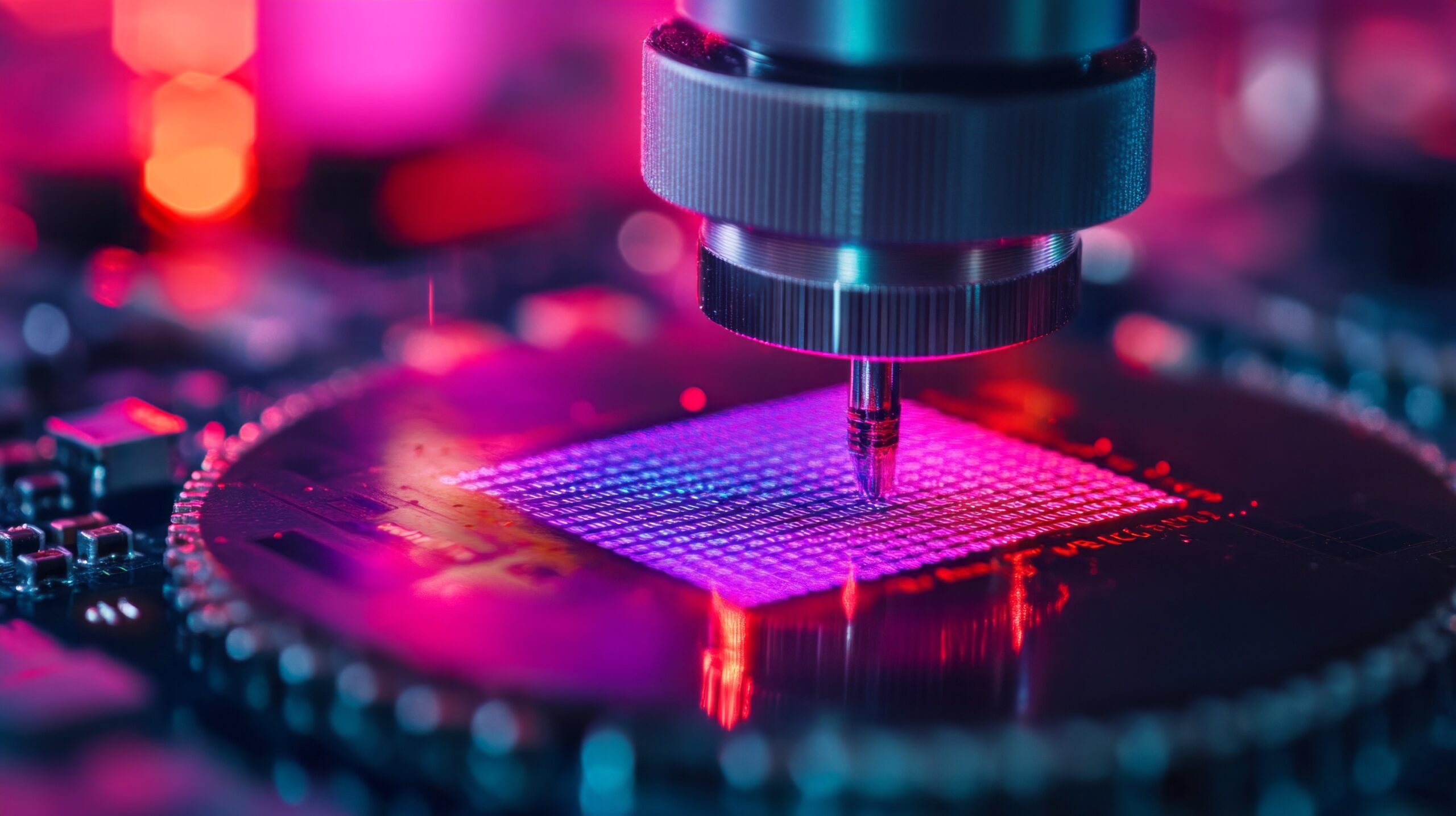
The Wide-Bandgap (WBG) Semiconductor Laboratory, led by Professors Zlatko Sitar and Ramón Collazo, pioneers research in the growth, characterization, and device integration of III-nitride and related wide-bandgap semiconductors. The team develops advanced methods for bulk and epitaxial crystal growth, polarity control, and defect management, enabling the development of next-generation optoelectronic and power devices.

Ramón Collazo, Principal Investigator
Collazo’s key research areas

Controlled Polarity Engineering in III-Nitrides

Bulk AlN Substrates and Epitaxial Growth

Characterization and Device Integration of Wide Bandgap Materials
Through innovations in aluminum nitride (AlN) crystal growth, lateral polarity engineering, and materials processing, the group advances the fundamental science and commercial applications of wide-bandgap materials—driving breakthroughs in deep-UV light sources, high-voltage electronics, and energy-efficient systems.
Zlatko Sitar, Principal Investigator

Sitar’s key research areas

AlN Crystal Growth and Commercialization

III-Nitride Epitaxy and Lateral Polarity Devices
Wide/Extreme Bandgap Semiconductors and Devices
Research Focus: Advancing Wide-Bandgap Semiconductor Materials and Devices
Our areas of expertise include:
- Epitaxial growth and materials development:
- Metal-organic chemical vapor deposition (MOCVD) of III-nitride semiconductors
- Bulk crystal growth of aluminum nitride (AlN) and gallium nitride (GaN)
- Defect reduction, polarity control, and doping engineering
- Alloy design for next-generation optoelectronic and power materials
- Characterization and device integration:
- Optical and electrical characterization of III-nitride materials
- Polarization and strain effects in wide-bandgap semiconductors
- High-power and high-frequency electronic devices
- Ultraviolet and deep-UV optoelectronic devices
- Core research goals:
- Advancing fundamental understanding of wide-bandgap materials
- Enabling scalable, high-quality nitride substrates and epitaxy
- Driving innovation in power electronics, solid-state lighting, and quantum technologies
Selected High-Impact Publications
- On the origin of the 265 nm absorption band in AlN bulk crystals — AP Letters
- Progress on n-type doping of AlGaN alloys on AlN single crystal substrates for UV optoelectronic applications — PSSC
- Universal phonon mean free path spectra in crystalline semiconductors at high temperature — Nature
- Growth of AlN/GaN layered structures by gas source molecular‐beam epitaxy — JVST B
- Growth of cubic phase gallium nitride by modified molecular-beam epitaxy — JVST A