We advance the science and technology of III-nitride and wide-bandgap semiconductor materials for optoelectronics, power devices and quantum systems. We aim to push the boundaries of crystal growth, polarity engineering, defect control and device integration, translating fundamental insights into practical photonic, UV and high-voltage applications.
Bulk and Epitaxial Growth of AlN/GaN Crystals and Films
We develop scalable methods to grow high-purity aluminum nitride (AlN) and gallium nitride (GaN) crystals and epitaxial films with low defect densities, optimized doping and controlled texture. Our innovations include plasma-assisted MBE, MOCVD and bulk boule growth techniques. These materials form the foundation for advanced device architectures in UV light sources and power electronics.
Polarity Engineering, Defect Control and Interface Design
Polarity (i.e. orientation of material crystal faces) plays a crucial role in device behavior. We manipulate polarity, strain and interfacial defects in heterostructures and lateral junctions to control carrier flow, reduce leakage and enhance performance. This thrust includes lateral homojunction devices, compositional grading and interface passivation strategies.
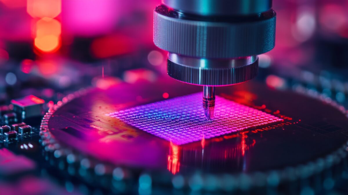
Device Integration, Characterization and Applications
We bridge materials with function by fabricating and testing devices such as UV LEDs, power diodes, deep-UV lasers and GaN transistors. Our characterization toolbox includes optical spectroscopy, high-resolution X-ray diffraction, electron microscopy, electrical transport and device testing under extreme conditions. We validate material advances in real-world device performance.
Methods and Capabilities
Crystal growth and epitaxy: plasma-assisted MBE, MOCVD, bulk boule growth
Structural and optical characterization: XRD, TEM, SEM, photoluminescence, cathodoluminescence
“The world is energetically more and more hungry, and the importance of integrating all the sources of energy will become a big problem; and this is where aluminum nitrate-based technology comes in as a superstar.”
Zlatko Sitar
Kobe Steel Distinguished Professor of Materials Science and Engineering Founder of Adroit Materials, Inc. and HexaTech, Inc.